 Español
Incluciencia: primera actividad de 2018 en colegio calasancio de Zaragoza
Incluciencia sigue en marcha. Ya no hay quien la pare. Nos hemos estrenado en Zaragoza en el colegio Calasancio- Escolapios Zaragoza. con alumnos de 3º y 4º ESO.
Actividades de ADN, Derechos Humanos, Matemáticas y Magia y el testimonio personal de Daniel Oliván, un ex-alumno del colegio apasionado por la mecánica han constituido las actividades del día.


 15
15Project INCLUCIENCIA to motivate students through science activities
INCLUCIENCIA is just born to prevent the increased dropping out of school.
INCLUCIENCIA is a project funded by FECYT and led by Jose Miguel González, which aims to reduce the Early School Leaving and lack of motivation of adolescents through scientific dissemination. Our goal is to motivate high school students using science as an empowerment tool. The methodology used pretends to attract the interest of students through lectures, workshops and experiments, and differs from similar activities in the fact that everything is related to possible professional opportunities that the person involved can choose. In addition, the project has methods of impact analysis and know-how to work with any adolescent group.
Those secondary schools interested in opening the doors to INCLUCIENCIA (free of charge), please contact ,
incluciencia@gmail.com
Last news reported in:
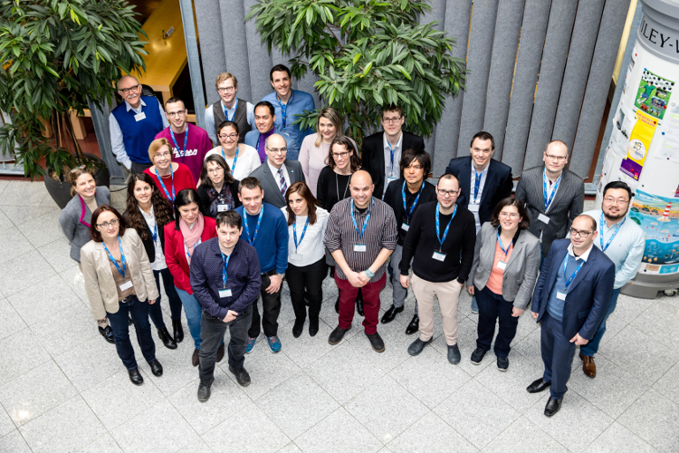
2018 Japanese-European EnEx Workshops エクセレンスの実現
![]() Our “Enabling Excellence” ITN project is organising six International Japanese-European Workshops in Japan between 21st and 30th May 2018, to promote the project’s network to Japanese Universities and companies. The workshops will include presentations from supervisors and students and visits to Japanese companies and universities.
Our “Enabling Excellence” ITN project is organising six International Japanese-European Workshops in Japan between 21st and 30th May 2018, to promote the project’s network to Japanese Universities and companies. The workshops will include presentations from supervisors and students and visits to Japanese companies and universities.

10alamenos9
10alamenos9 Festival Nano.
We participated in the event Festival NANOin Caixaforum Zaragoza. Nano-seminars, Nano-dialogs, and nano-workshops for High School children .
10th and 11th of April in zaragoza.


RAMAN DAY 2018.
RAMAN DAY 2018. Avances y Aplicaciones en Espectroscopía Raman
José Miguel González selected to attend the first CHEMPUBSOC EUROPE YOUNG RESEARCHERS MEETING
CHEMPUBSOC EUROPE YOUNG RESEARCHERS MEETING.
8th-9th March. Weinheim (Germany). Wiley editorial site
Jose Miguel Gonzalez was one of the invited young european scientist attending the event organized by the ChemPubSoc Europe.
Yesterday was the start of the 1st ChemPubSoc Europe Early Career Researchers Meeting. It brought together the next…
Publicada por ChemistryViews en viernes, 9 de marzo de 2018
ChemPubSoc Europe Hosts Young Researcher Workshop
Celera Note (spanish):
http://www.acelerame.org/chempubsoc-europe-young-researche…/
Conferencia en el ICB: Monitoring the integration process of individual single-walled carbon nanotubes into sensing devices
El Dr. Miro Haluska de Micro and Nanosystems ETH en Zurich, Suiza dará una conferencia el 13 de Julio en el ICB-CSIC: Monitoring the integration process of individual single-walled carbon nanotubes into sensing devices.
El Seminario tendrá lugar en el salón de actos del ICB-CSIC, Zaragoza.
Jueves 13 de Julio, 12:30
RESUMEN:
Monitoring the integration process of individual single-walled carbon nanotubes into sensing devices
Miro Haluska, Wei Liu, Sebastian Eberle, Lalit Kumar, Laura Vera Jenni, Pooriya Gh Ghanbari, Pol Peiffer, Cosmin Roman, Christofer Hierold. Micro and Nanosystems ETH Zürich, Tannenstrasse 3, 8092 Zurich, Switzerland
Our nanotube devices (gas sensors and nanoresonators) are based on individual single-walled carbon nanotubes (SWCNTs) and were fabricated either by standard photo- or electron-beam lithography, or by ultra-clean mechanical transfer from dedicated growth substrates onto the final devices [1]. SWCNTs were synthesized on SiO2/Si chips or SOI structures from ferritinbased Fe catalyst nanoparticles by LPCVD at 850°C in CH4/H2 [2]. As-grown suspended SWCNTs were visualized by post-synthesis deposition of volatile nanoparticles and inspected by optical microscopy and by Raman spectroscopy. For the optical microscopic visualization we used a para-nitrobenzoic acid (pNBA) based approach as introduced in [3]. Substrate bound CNTs were pre-characterized by AFM and Raman spectroscopy. The combination of this visualization and characterization methods allows for the determination of the position of CNTs with respect to predefined chip structures and the selection of pre-characterized nanotubes for further device fabrication.
Devices based on individual SWCNTs often do not perform as expected from nanotubes’ outstanding intrinsic properties. Additionally, variations in electrical characteristics of individual carbon nanotube field effect transistors (iCNFETs), cannot be explained solely by the variation in intrinsic properties of different SWCNTs [4]. Both above-mentioned observations can be caused by physical and chemical impacts of device fabrication processes on SWCNTs. To monitor the impact of the device fabrication, selected SWCNTs were characterized by Raman spectroscopy after individual processing steps. By this approach we determined, for example, the minimum thickness of sacrificial alumina layer required to protect SWCNTs from the impact of plasma ashing used for removing lithography resist residuals [5]. Using the process flow monitoring for optimization of the device fabrication helped narrowing the variation of devices resistance and 1.8 times improvement in median value of device resistance.
References:
- Muoth, M., Hierold, C., (2012). Transfer of carbon nanotubes onto microactuators for hysteresisfree transistors at low thermal budget. IEEE MEMS 2012, Paris, pp 1352-1355.
- Durrer, L., Greenwald, J., Helbling, T., Muoth, M., Riek, R., Hierold, C., (2009). Narrowing SWNT diameter distribution using size-separated ferritin-based Fe catalysts. Nanotechnology 20, 355601-7
- Zeevi, G., et al., (2016) Automated circuit fabrication and direct characterization of carbon nanotube vibrations. Nature Comms. Art Nr.: 12153, DOI: 10.1038/ncomms12153.
- Park, H., Afzali, A., Han S.J., Tulevski, G.S., Franklin, A.D., Tersoff, J., Hannon J.B., Haensch, W., (2012). High-density integration of carbon nanotubes via chemical self-assembly. Nature nanotechnology 7, 787-791.
- Liu, W., Chikkadi, K., Hierold, C., Miroslav Haluska, (2016) Enabling fabrication of clean electrical contacts to carbon nanotubes using oxygen plasma ashing. physica status solidi b, 253, 2417-2423.
Manuela Meloni (Univ. Sussex) visit the G-CNN group
Manuela Meloni from University of Sussex carried out his secondment stay in our group (jun 2017). Closely working with Sandra, Emin and Lorenzo she worked on the synthesis of graphite oxide and on the synthesis of polymer composites with graphene. Work will continue at Univ. Sussex/ICB.
We are already thinking in future collaborations.


